

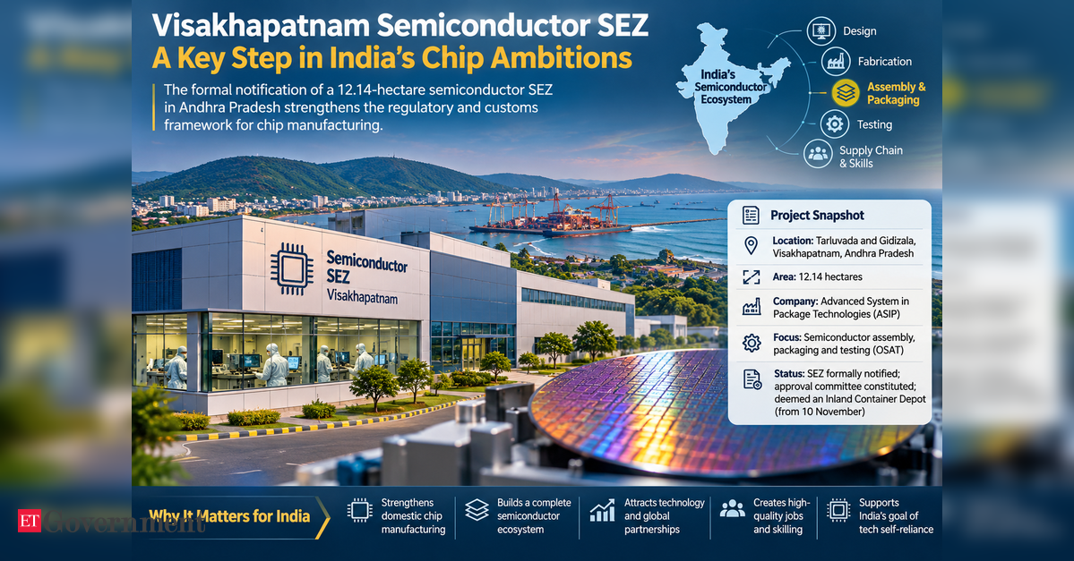
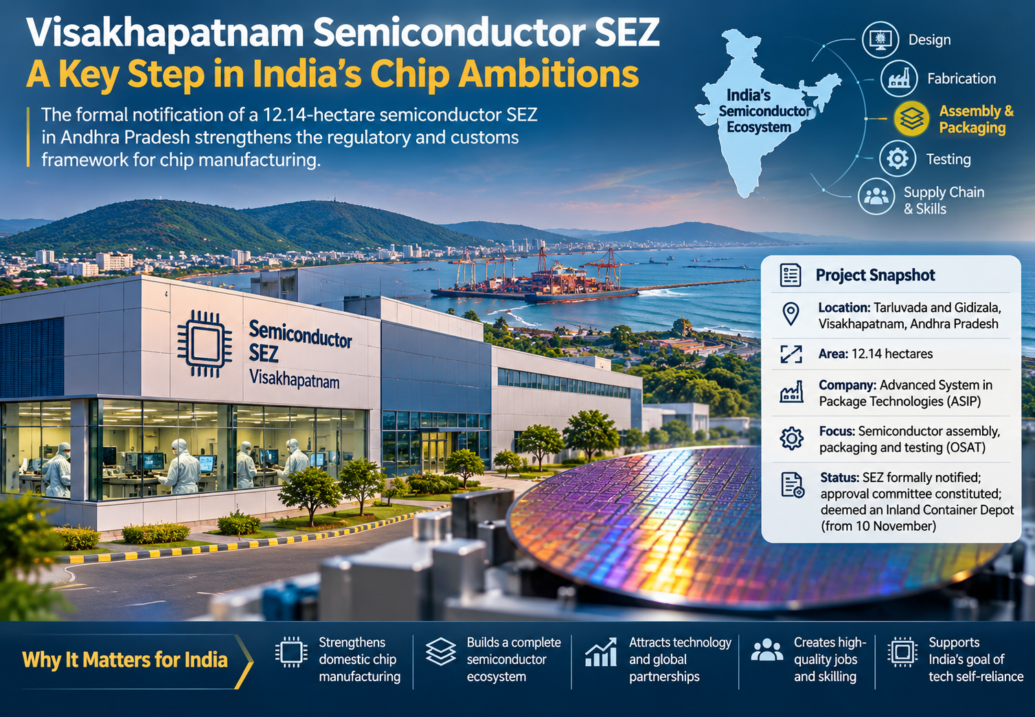
India’s ambition to emerge as a global semiconductor manufacturing hub has received another institutional boost with the Union government’s formal notification of a Special Economic Zone (SEZ) for semiconductor manufacturing in Visakhapatnam, Andhra Pradesh. Although the notified area covers just 12.14 hectares, the development carries significance beyond its geographical size.It represents another step in India’s attempt to build a domestic semiconductor ecosystem capable of reducing import dependence, attracting international technology partnerships and participating in global electronics supply chains.The Ministry of Commerce and Industry, through notification S.O. 6148(E), dated November 10 and published on November 13, designated land in Tarluvada and Gidizala villages of Anandapuram mandal as an SEZ for Advanced System in Package Technologies Private Limited (ASIP).The government had issued the letter of approval on October 19. The notification also constitutes an Approval Committee and designates the SEZ as an Inland Container Depot under the Customs Act, effective November 10. These are statutory measures facilitating the project’s implementation, rather than announcements of fresh investment.The project is important because ASIP is developing an outsourced semiconductor assembly and test (OSAT) facility, a segment that forms an essential link between semiconductor wafer fabrication and the supply of finished chips to electronics manufacturers. While fabrication produces semiconductor circuits on silicon wafers, packaging and testing protect the chips, establish electrical connections and verify their performance before commercial deployment.India’s semiconductor strategy cannot succeed through fabrication plants alone. It requires an integrated industrial ecosystem comprising chip design, wafer manufacturing, assembly, packaging, testing, specialised materials, precision equipment and skilled personnel. The Visakhapatnam project addresses one part of this larger industrial requirement.The Andhra Pradesh government had earlier approved land allotment for ASIP’s project, with a proposed investment of approximately ₹2,388 crore in two phases and an employment potential of around 1,000 people. The project has received support under the India Semiconductor Mission. These investment figures relate to the previously approved project and should not be interpreted as new commitments arising from the November SEZ notification.The company’s technological ambitions extend beyond conventional chip assembly. In an interview with EE Times published in August 2026, ASIP Technologies CEO Venkata Simhadri outlined plans to begin with flip-chip ball-grid array packaging and wire-bond technologies, while pursuing more sophisticated 2.5D packaging capabilities.“I want to have a 2.5D technology in production in our plant in Visakhapatnam by 2030 the earliest. That is my target,” Simhadri said. The company is working with South Korean semiconductor packaging specialist APACT, bringing international technological experience into the proposed Indian facility.This progression matters because advanced packaging is becoming increasingly important to semiconductor performance. Modern computing systems increasingly depend on combining multiple semiconductor components within sophisticated packages rather than relying exclusively on improvements in individual silicon chips. Developing these capabilities could eventually help Indian manufacturers participate in higher-value segments of the global semiconductor industry.The project also fits into the government’s broader semiconductor strategy. In July 2026, the Union Cabinet approved Semicon 2.0 with an outlay of ₹1,27,500 crore, targeting chip design, manufacturing equipment, materials, fabrication, advanced packaging, research and workforce development. According to official figures released in July, 12 semiconductor manufacturing units had been approved under the earlier programme, representing investments exceeding ₹1.64 lakh crore. Nine of these were packaging facilities.Union Electronics and Information Technology Minister Ashwini Vaishnaw, speaking at SEMICON India 2026 in September, emphasised that the next phase of India’s semiconductor development must create an entire industrial ecosystem rather than merely establish individual factories. He identified domestic capabilities in equipment, chemicals, gases, precision manufacturing and specialised materials as essential to long-term competitiveness.The Visakhapatnam SEZ’s customs designation is particularly relevant to this objective. Semiconductor facilities depend on internationally sourced machinery, specialised materials and components, frequently moving across borders during different stages of production. An established customs framework can support these operations, although the ICD designation does not itself establish additional fiscal concessions or guarantee faster clearances.Nevertheless, several challenges remain. India’s semiconductor packaging industry continues to depend heavily on imported substrates, lead frames, moulding compounds and specialised equipment. Simhadri acknowledged in his EE Times interview that domestic sourcing of several essential packaging inputs was effectively nonexistent, while expressing expectations that localisation could reach 20–30 per cent within three to four years.Technology transfer presents another challenge. International partnerships can accelerate manufacturing capability, but sustained competitiveness requires Indian engineers and companies to acquire expertise in package design, process engineering, reliability testing and advanced materials. Without these capabilities, India risks becoming predominantly an assembly destination rather than a significant contributor to semiconductor technology development.There is also the question of commercial viability. Semiconductor manufacturing demands exceptionally high precision, consistent production yields, reliable electricity, cleanroom infrastructure and internationally competitive costs. Government incentives can reduce initial investment risks, but long-term success depends on securing customers and delivering products that meet demanding global standards.The notification does not establish that the facility has begun commercial production. Its ultimate significance will depend on construction progress, equipment installation, customer qualification and the ability to achieve sustained manufacturing volumes.For India, the larger opportunity is to connect its established strength in semiconductor design with domestic manufacturing and packaging capabilities. The Visakhapatnam project could contribute to that transition, particularly if it develops local suppliers, skilled engineers and higher-value packaging technologies.The country’s semiconductor ambitions will ultimately be judged not by the number of projects announced or zones notified, but by the chips manufactured, technologies mastered and supply chains established. Visakhapatnam represents another step towards that objective. Whether it becomes a competitive semiconductor manufacturing centre will depend on what happens after the regulatory approvals.
