India has crossed the first threshold of its semiconductor ambition: global and domestic companies are investing, fabrication and packaging plants are taking shape, and billions of rupees in public incentives have been committed.
Semicon 2.0 now confronts the more difficult question—what will India actually get in return for ₹1.27 lakh crore of taxpayer-backed support?
The answer cannot be measured simply by counting approved projects or investment announcements. The real test will be whether subsidies translate into operational fabs, Indian suppliers, technology capabilities, skilled engineers, locally developed intellectual property and progressively higher domestic value addition.
In other words, India’s semiconductor mission is moving from the task of attracting investment to the more complex challenge of governing an industrial ecosystem.
That makes Semicon 2.0 fundamentally different from the first phase of the India Semiconductor Mission. The initial challenge was to convince companies that India could become a credible semiconductor manufacturing destination. The next challenge is considerably more complex: coordinating the Ministry of Electronics and Information Technology (MeitY), India Semiconductor Mission (ISM), state governments, utilities, research institutions, universities and private investors while ensuring that large public incentives are linked to measurable technological and economic outcomes.
The government on August 31 notified all six pillars of Semicon 2.0, following the Union Cabinet’s approval of the ₹1,27,500-crore programme in July. The six pillars cover chip design, semiconductor equipment and materials, fabrication facilities, ATMP/OSAT and advanced packaging, research and development, and talent development.
The crucial question is therefore shifting from “How many semiconductor projects can India attract?” to “How much semiconductor capability can India actually create?”
From factories to an ecosystem
Semicon 1.0, launched with an outlay of ₹76,000 crore, had to overcome a fundamental credibility problem: could India persuade companies to make multibillion-dollar semiconductor investments in a country without an established fabrication ecosystem?
There has been measurable progress. Twelve semiconductor manufacturing units involving cumulative investment of more than ₹1.64 lakh crore have been approved. These include a silicon fab, a silicon-carbide fab, an integrated gallium-nitride Micro LED display fab and nine packaging units. Micron, Kaynes and CG Semi have commenced commercial production, while India’s first major semiconductor fab is scheduled to be commissioned in 2028.
Semicon 2.0 confronts a different problem. A semiconductor factory cannot become globally competitive simply because its building and machinery are located in India. It depends on an intricate network of specialty chemicals, ultra-pure gases, wafers, sophisticated manufacturing equipment, spare parts, clean-room infrastructure, precision engineering, testing, logistics, reliable electricity, water and highly specialised human capital.
This explains the new emphasis on machines and materials. Companies involved in manufacturing and R&D of semiconductor equipment and in producing materials, chemicals and gases will receive support. The objective is not merely import substitution but the creation of Indian suppliers capable of integrating into global semiconductor supply chains.
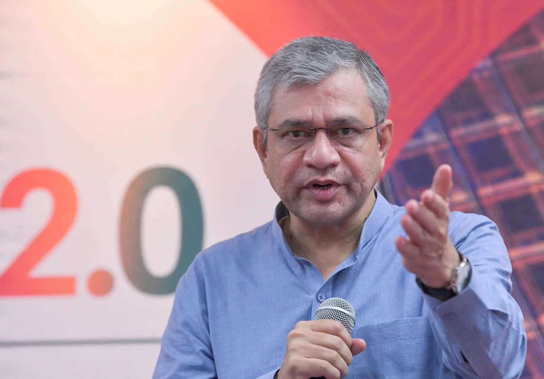
Electronics and IT Minister Ashwini Vaishnaw indicated the scale of this ambition while announcing the detailed framework. “Over the next few months, almost every major semiconductor equipment manufacturer will be setting up a base, and supply chains in India,” he said, adding that Indian manufacturers of components and precision equipment could become suppliers to these global equipment companies.
“Now the time is ripe to move to next stage to develop semiconducor ecosystem through Semicon 2.0. The objective of the scheme is self reliance and fostering a globally competitive industry,” IT Secretary S. Krishnan said at a briefing.
The governance challenge consequently extends far beyond MeitY and ISM. State governments control critical components of land, infrastructure, local incentives and clearances. Utilities must provide exceptionally reliable power and enormous quantities of high-quality water. Universities and research institutions have to supply specialised talent. International partners remain important for process technologies and equipment, while private companies must invest over technology cycles extending several years.
Semiconductor policy is therefore becoming a coordination challenge as much as a subsidy programme.
How should ₹1.27 lakh crore be governed?
The structure of Semicon 2.0 suggests that the government is attempting to differentiate incentives according to technologies and strategic requirements.
Large silicon wafer fabrication projects can receive central fiscal support of 40 per cent of eligible capital expenditure. Compound semiconductor and specialised fabs can receive support of 35 per cent. Advanced semiconductor packaging projects can similarly receive support of up to 35 per cent, while conventional packaging attracts lower support. Incentives are to be disbursed on a pari-passu basis, linking government payments to actual capital investment by the companies.
This differentiation matters because the economic and strategic value of semiconductor projects varies dramatically. A sophisticated wafer fab, an advanced packaging facility and a conventional assembly operation cannot be evaluated merely by comparing headline investment or employment numbers.
ISM’s appraisal standards will therefore become critical. Proposals need to be assessed not only for financial viability but for technological relevance, execution capability, global competitiveness and their ability to deepen the Indian semiconductor ecosystem.
The government will also have to maintain a delicate balance between speed and scrutiny. Semiconductor investments are globally competitive: excessive procedural delays can push projects towards other jurisdictions. But the scale of public support means that accelerated approval cannot come at the cost of rigorous technical and financial appraisal.
The principle should be straightforward: the greater the public incentive, the clearer the milestones and measurable outcomes should be.
Measuring domestic value addition
The larger question is what India receives in exchange for its fiscal support.
The most visible metrics—investment committed, factories approved and jobs generated—are useful but incomplete. Semicon 2.0 should increasingly be evaluated through indicators such as domestic procurement of equipment and materials, development of Indian suppliers, locally generated intellectual property, engineering capabilities created, export revenue, advanced packaging capability and the proportion of manufacturing inputs sourced domestically.
This is particularly important because semiconductor supply chains are among the world’s most internationally distributed industrial systems. A plant physically operating in India could still depend overwhelmingly on imported manufacturing equipment, chemicals, wafers, intellectual property and process technologies.
The government’s own articulation of Semicon 2.0 places greater domestic value addition and supply-chain resilience among its objectives.
But localisation should not become a mechanical percentage exercise. No major semiconductor economy produces every piece of equipment or every material domestically. India’s objective should instead be to identify parts of the value chain where domestic capability is commercially viable, technologically achievable or strategically indispensable.
That could include specialty materials, industrial gases, components for semiconductor equipment, chip design, compound semiconductors, advanced packaging and selected manufacturing technologies.
The quality of domestic value addition matters as much as the quantity. Manufacturing a low-value component locally cannot be treated as equivalent to acquiring proprietary process technology, developing semiconductor IP or creating a globally competitive equipment supplier.
Talent cannot be measured by numbers alone
Human capital is another area where the government sees significant early momentum. On August 31, Vaishnaw said India had achieved its target of developing 85,000 semiconductor engineers—originally envisaged over ten years—in four years. The government has now set a target of developing another one lakh semiconductor engineers.
“Students from Tier-II and Tier-III cities have designed more than 250 semiconductor chips,” Vaishnaw said. The government also expects India’s expanding semiconductor ecosystem to generate tens of thousands of direct jobs.
Earlier government data showed that around 68,000 people had been trained under semiconductor-related initiatives, while 175 designs had been taped out from SCL Mohali. New semiconductor curricula and access to sophisticated Electronic Design Automation tools have also expanded training capacity across engineering institutions.
But numbers trained cannot become the primary success metric. The more difficult shortages may emerge in experienced process engineers, equipment technicians, clean-room specialists, materials scientists, packaging experts and fab-construction professionals.
Semicon 2.0 recognises this by proposing greater industry involvement in training for clean rooms, fab construction and other specialised ecosystem requirements.
Moving up the technology curve
The R&D challenge may prove even more consequential. India’s semiconductor manufacturing journey has initially concentrated largely on the 28nm–110nm technology range. Under Semicon 2.0, the government intends to work with leading Indian and international research institutions to develop more advanced nodes and technologies.
This is important because semiconductor competitiveness is ultimately determined not merely by manufacturing capacity but by the ability to absorb, improve and eventually develop technology.
India already possesses a substantial semiconductor design workforce. Under the first mission, 24 semiconductor design projects from startups and MSMEs received financial support, while 105 startups and MSMEs obtained access to industry-standard EDA tools. These companies are working on chips and systems for applications ranging from drones and satellite communications to AI, telecom equipment, surveillance cameras and smart meters.
Semicon 2.0 must connect this design capability more closely with manufacturing, packaging, materials and research. Otherwise India risks developing several successful but disconnected pieces of the semiconductor value chain. That is why institutional coordination may ultimately matter as much as the quantum of subsidies.
The first phase of India’s semiconductor mission was largely about proving that India could attract serious semiconductor investment. The second must demonstrate that these investments can create durable technological capability.
The scoreboard must consequently change—from rupees sanctioned to fabs commissioned, from companies subsidised to suppliers created, from engineers trained to expertise acquired, from imported equipment to Indian precision-manufacturing capability, and from chips packaged in India to intellectual property and advanced technologies developed here.
Industry expectations are already substantial. India Electronics and Semiconductor Association President Ashok Chandak has estimated that, given the investment pipeline and expanded scope of Semicon 2.0, the programme could catalyse more than ₹5 lakh crore of cumulative private and industry investment over the next five to seven years.
If that scale of investment materialises, the government’s role will increasingly change from promoter to ecosystem governor.
With ₹1.27 lakh crore of public resources potentially involved, Semicon 2.0 is therefore much more than another semiconductor subsidy programme. It is a test of whether India can execute strategic industrial policy with technological judgement, federal coordination, fiscal discipline and measurable accountability.
Semicon 1.0 demonstrated that India could get semiconductor factories onto investment plans and, increasingly, onto the ground. Semicon 2.0 must accomplish something harder: ensure that those factories become anchors for technology, talent, suppliers and intellectual property.
The ultimate measure of success will not be how much subsidy India distributes, but how much semiconductor capability remains when the subsidy is no longer necessary.